

SLL's embedded software innovation has been recognised by our customers and partners. Major FPGA, memory, and development board makers now officially partner with SLL. This ensures SLL IP is validated on a wide range of physical devices. SLL customers are located in most geographical regions, and include Fortune Global 500's, government agencies, and SME's from USA and Canada to China.

xSPI Multiple Bus Memory Controller (xSPI-MBMC)
The industry ‘defacto standard’ memory controller for xSPI-like memories
Product page for
OctaFlash, OctaRAM, Octal RAM, OctaMCP and Octal MCP
PSRAM and NOR Flash devices
SLL collaborates closely with all OctaBus memory vendors.
SLL partners and supported OctaBus and Octal Bus memory device vendors
SLL collaborates closely with Macronix
SLL’s IP supports Xilinx FPGA devices
SLL is JSC’s partner
SLL is Trenz Electronic’s partner
SLL is a Microchip (Microsemi) CompanionCore Partner
MBMC product overview
SLL’s xSPI Multiple Bus Memory Controller (MBMC) IP provides full support for:
- Macronix® OctaBus™ / OctaFlash™ (NOR Flash)
- AP Memory® OctaRAM™
- Integrated Silicon Solution Inc.® (ISSI) x8 Octal RAM and Octal RAM with inbuilt ECC
- Jeju Semiconductor Corp® (JSC) OctaRAM™
The low pin count (11 to 12 user I/O pins) memories offer good performance with lower hardware and power costs. Memory device variants offer up to 256 Mbit PSRAM, up to 2 Gigabit NOR Flash, up to 200 MHz DDR clock speeds, with a x8 wide data path, and {6 mm x 8 mm} and {8 mm x 8 mm} BGA24 package options.
SLL is the official partner with all the above memory vendors. SLL works closely with our partners to ensure SLL’s memory controllers are physically qualified with their memory device variants, significantly reducing your project’s risks.
SLL’s small MBMC IP v3.2.x enables you to easily evaluate, select and adopt the benefits of the latest x8 OctaFlash, OctaRAM and Octal RAM memories in your projects and products.
SLL provides world class pre-sales and post-sales technical support for all the major memory vendors and FPGA vendors, helping you navigate the rapidly evolving market, on the platform of your choice.
Get to market faster, with lower power consumption, lower pin count, lower cost, and far lower project risk by using SLL’s memory controller in your project/s.
xSPI MBMC support for FPGA and ASIC targets
This memory controller IP has been ported to, and physically tested on, a broad range of FPGA device variants, including:
- Most modern Intel FPGA device families, including:
- Intel MAX 10 – Up to 200 MHz DDR
- Cyclone IV
- Cyclone 10 LP – Up to 200 MHz DDR
- Cyclone 10 GX – Up to 250 MHz DDR
- Cyclone V
- Cyclone V SoC
- Arria 10 – Up to 250 MHz DDR
- Arria 10 SoC – Up to 250 MHz DDR
- Stratix 10 – Up to 250 MHz DDR
- Most modern Xilinx FPGA device families, including:
- Artix-7
- Kintex-7
- Virtex-7
- Zynq 7000
- Kintex Ultrascale+
- Zynq Ultrascale+
- Virtex Ultrascale+ (ideal for supporting ASIC design prototyping in FPGA)
- Microchip (Microsemi)
- PolarFire FPGA – Up to 250 MHz DDR
Other FPGA device families may be available on request. Please contact SLL at info@synaptic-labs.com with details about the specific currently unsupported FPGA device family that you would like to use.
This memory controller IP is also currently being ported from FPGA to standard cell ASIC at up to 250 MHz DDR with x4/x8/x16 datapath support.
xSPI MBMC Trials
To request a trial for selected FPGA device families, please visit here.
xSPI MBMC Capabilities
- Includes tight integration with all the major FPGA vendor’s graphical system integration tools (Platform Designer, Vivado, …)
- Features high quality local interconnect, with support for the following interconnect protocols:
- ARM AMBA AXI4 protocol
- ARM AMBA APB3 protocol
- Intel Avalon-MM protocol
- other interconnect protocols available on request…
- Includes internal clock-crossing circuitry between the local bus interconnect and the external memory channel to reduce circuit area and improve the performance of the customer’s design
- Excellent memory access performance for both latency sensitive and bandwidth intensive applications:
- The round trip time for read memory transfer requests through the memory controller has been optimized for latency sensitive applications, such as processor cores.
- The memory controller supports long burst memory transfer requests over the memory channel to sustain high effective memory bandwidth (>90% efficiency of memory channel)
- Note: SLL offers a range of cache technologies to significantly increase the performance of processor cores that do not have internal instruction and/or data caches when accessing external memories.
- Features low circuit area and low SRAM usages, making SLL’s memory controller viable for use in resource constrained designs.
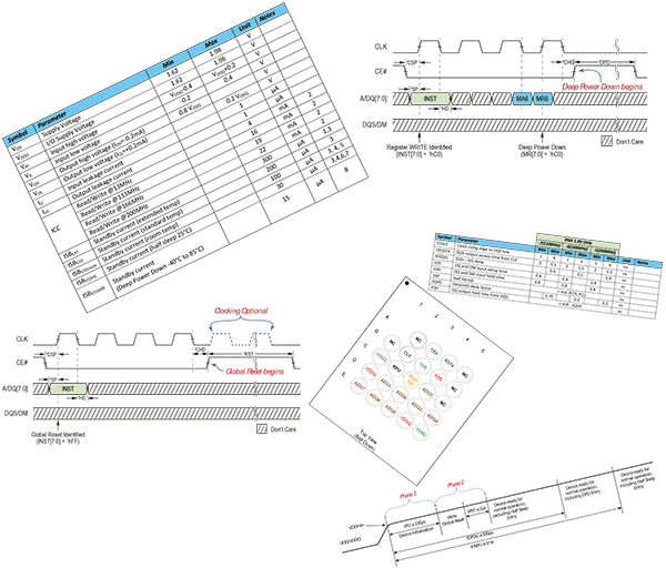
- Includes optional support for automatic configuration of memory devices at power on:
- FPGA customers typically use the automatic configuration option
- This dramatically simplifies integration of SLL’s memory controller in customer designs, enabling all firmware to be executed in place from x8 NOR Flash.
- Include support for manual configuration of the memory controller and any attached memory devices
- ASIC customers typically use the manual configuration option
- ASIC customers can prototype their designs in FPGA with manual configuration option enabled
- Supports x4, x8 and x16 data path width in a single instantiation of SLL’s memory controller IP
- Supports 2 or more instantiations of the memory controller IP in one project
- Preliminary support for splitting AXI4 requests across 2 instances of the memory controller in parallel to double memory bandwidth is now available
xSPI MBMC markets, applications and use cases
Customers include industrial consortia, high profile government scientific organisations, universities, Fortune Global 500’s down to SME’s around the globe, from USA to China. Applications include commercial and industrial projects and products, such as: Sensors, video, industrial automation, medical, transport, photonics, … Use cases include: eXecution in Place (XiP) of software, long burst DMA access, video frame buffering, packet buffering, …
xSPI MBMC OctaBus memory devices
xSPI MBMC support for Macronix OctaBus™
Status of Macronix OctaBus™ device testing and qualification performed by SLL:
- Macronix International Co., Ltd – OctaBus™:
- Physically validated on Trenz board:
- MX25UM512 (512 Mbit, 1.8V)
- Physical validation in process on Trenz board:
- MX25LM51245GXDI00 (512 Mbit, 3V)
- MX25UM51245GXDIH0 (512 Mbit, 1.8V)
- MX25UM51345GXDI00 (512 Mbit, 1.8V)
- MX25UW51345GXDI00 (512 Mbit, 1.8V)
- MX66LM1G45GXDI00 (1024 Mbit, 3V)
- MX66UM1G45GXDI00 (1024 Mbit, 1.8V)
- MX66UM2G45GXRI00 (2048 Mbit, 1.8V)
- Physically validated on Trenz board:
xSPI MBMC support for AP Memory OctaRAM
Status of AP Memory IoT (OctaRAM) device testing and qualification performed by SLL:
- AP Memory – IoT (OctaRAM):
- Physically validated:
- APM6408L-OC (64 Mbit, 1.8V)
- APM6408L-3OC (64 Mbit, 3.0V)
- Physically validated on Trenz board:
- APS6408L-30C (64 Mbit, 3.0V)
- Validation pending:
- APS25608N‐OCx (256 Mbit, 1.8V)
- APS51208N‐OCx (512 Mbit, 1.8V)
- Physically validated:
xSPI MBMC support for ISSI Octal RAM
Status of ISSI Octal RAM device testing and qualification performed by SLL:
- Integrated Silicon Solution Inc. (ISSI) – Octal RAM:
- Physical validation in process on Trenz board:
- IS66WVO16M8DALL-200BLI (128 Mbit, 1.8V)
- IS66WVO16M8DBLL-100BLI (128 Mbit, 3V)
- IS66WVO16M8DBLL-133BLI (128 Mbit, 3V)
- IS66WVO16M8EDALL-166BLI (128 Mbit, 1.8V, with ECC)
- IS66WVO16M8EDBLL-133BLI (128 Mbit, 3V, with ECC)
- IS66WVO32M8DALL-200BLI (256 Mbit, 1.8V)
- IS66WVO32M8DBLL-133BLI (256 Mbit, 3V)
- IS72WVO32M8AWO256-200HLA2 (256 Mbit Octal Flash, 256 Mbit Octal RAM, 1.8V)
- IS72WVO32M8BLO256-133HLA2 (256 Mbit Octal Flash, 256 Mbit Octal RAM, 3V)
- Support planned:
- IS67WVO16M8DALL
- IS67WVO16M8DBLL
- IS67WVO16M8EDALL (with ECC)
- IS67WVO16M8EDBLL (with ECC)
- IS67WVO32M8DALL
- IS67WVO32M8DBLL
- Physical validation in process on Trenz board:
xSPI MBMC support for ISSI Octal MCP
Status of ISSI Octal RAM device testing and qualification performed by SLL:
- Integrated Silicon Solution Inc. (ISSI) – Octal MCP:
- Physical validation in process on Trenz board:
- IS72WVO32M8AWO256-200HLA2 (256 Mbit Octal Flash, 256 Mbit Octal RAM, 1.8V)
- IS72WVO32M8BLO256-133HLA2 (256 Mbit Octal Flash, 256 Mbit Octal RAM, 3V)
- Physical validation in process on Trenz board:
xSPI MBMC support for JSC OctaRAM
Status of JSC OctaRAM device testing and qualification performed by SLL:
- Jeju Semiconductor Corp (JSC) – OctaRAM:
- Physically validated:
- JSC28SSP8AGDY-50I (128 Mbit, 1.8V)
- JSC64SSP8AGDY-50I (64 Mbit, 1.8V)
- Physical validation in process on Trenz board:
- JSC28SSP8AGDY-50I (128 Mbit, 1.8V)
- JSC64SSP8AGDY-50I (64 Mbit, 1.8V)
- JSC64SSP8AGDY-75I (64 Mbit, 3V)
- Validated in simulator:
- JSC28SSU8AGDY-75I (128 Mbit, 3V)
- JSC64SSU8AGDY-75I (64 Mbit, 3V)
- Physically validated:
xSPI MBMC support for Commercial-off-the-shelf (COTS) boards
SLL has the broadest range of xSPI and xSPI-like board partners in this memory controller market. SLL has also tested our memory controller on the broadest range of COTS and proprietary boards in the market.
SLL leverages our close relationships to deliver known-working reference designs with trial copies of xSPI MBMC (that do not expire) to: (a) reduce your project risk; and (b) get you to market faster. SLL’s board partners include:
- Trenz Electronic GmbH
- Aries Embedded GmbH
- Devboards GmbH
- Intel Corporation (Intel PSG)
- Microsemi Corporation a wholly owned subsidiary of Microchip Technology Inc. (Microsemi)
SLL has also run our memory controller IP on boards from other board vendors such as:
Notice to Hardware Developers using xSPI MBMC
- Please validate your pin-mapping and PCB Layout for you selected memory devices with Synaptic Laboratories at info@synaptic-labs.com before manufacturing your first prototype to reduce risks.
- Please email info@synaptic-labs.com for SLL’s guidance with regard to supporting specific FPGA device families.
Macronix OctaBus™ Memory Resources
- Macronix International Co., Ltd
- Macronix OctaBus™ memory product page (LM/LW/UM/UW)
- Standards
- Macronix OctaBus™
- JEDEC JESD251 – EXpanded Serial Peripheral Interface (xSPI) for Non Volatile Memory Devices, Version 1.0
- JEDEC JESD216D – Serial Flash Discoverable Parameters (SFDP)
- Application notes and other guidance:
- Contact Macronix.
- Data sheet
- MX25LM
- MX25LM12845G ( 128 Mbit, 3.0V)
- MX25LM25645G ( 256 Mbit, 3.0V)
- MX25LM51245G ( 512 Mbit, 3.0V)
- MX25LW
- MX25LW51245G ( 512 Mbit, 3.0V)
- MX25UM
- MX25UM12845G ( 128 Mbit, 1.8V)
- MX25UM25345G ( 256 Mbit, 1.8V)
- MX25UM25645G ( 256 Mbit, 1.8V)
- MX25UM51245G ( 512 Mbit, 1.8V)
- MX25UM51245G-EX ( 512 Mbit, 1.8V)
- MX25UM51345G ( 512 Mbit, 1.8V)
- MX25UW12345G ( 128 Mbit, 1.8V)
- MX25UW
- MX25UW12845G ( 128 Mbit, 1.8V)
- MX25UW12A45G ( 128 Mbit, 1.8V)
- MX25UW25345G ( 256 Mbit, 1.8V)
- MX25UW25645G ( 256 Mbit, 1.8V)
- MX25UW51245G ( 512 Mbit, 1.8V)
- MX25UW51345G ( 512 Mbit, 1.8V)
- MX25UW6345G ( 64 Mbit, 1.8V)
- MX25UW6445G ( 64 Mbit, 1.8V)
- MX66LM
- MX66LM1G45G ( 1024 Mbit, 3.0V)
- MX66LM2G45G ( 2048 Mbit, 3.0V)
- MX66LW1G45G ( 1024 Mbit, 1.8V)
- MX66LW
- MX66LW2G45G ( 2048 Mbit, 1.8V)
- MX66UM
- MX66UM1G45G ( 1024 Mbit, 1.8V)
- MX25LM
AP Memory IOT RAM (OctaRAM) Resources
- AP Memory
- Standards
- Macronix Octabus Standard for OctaRAM
- Application notes and other guidance
- AP Memory, “OPI 24B/90B board design guide”, 5 March 2019.
- Request guidance by email
- AP Memory, “OPI 24B/90B board design guide”, 5 March 2019.
- Data sheets:
- APS-OC
- APS6408L-OC (64 Mbit, 1.8V)
- APS6408L-OC (bare die)
- APS6408L-OCX (bare die)
- APS6408L-OC-BA (6mmx8mm 24BGA)
- APS6408L-OCX-BA (6mmx8mm 24BGA)
- APS25608N‐OCx (256 Mbit, 1.8V)
- APS25608N-OCH (bare die)
- APS25608N-OCHX (bare die)
- APS25608N-OCH-BA (6mmx8mm 24BGA)
- APS25608N-OCH-BA (6mmx8mm 24BGA)
- APS51208N‐OCx (512 Mbit, 1.8V)
- APS51208N-OCH (bare die)
- APS51208N-OCHX (bare die)
- APS51208N-OCH-BA (6mmx8mm 24BGA)
- APS51208N-OCH-BA (6mmx8mm 24BGA)
- APS6408L-OC (64 Mbit, 1.8V)
- APS-3OC
- APS6408L-3OC (64 Mbit, 3.0V)
- APS6408L-3OC-BA (6mmx8mm 24BGA)
- APS6408L-3OCX-BA (6mmx8mm 24BGA)
- APS6408L-3OC (64 Mbit, 3.0V)
- APS-OC
ISSI Octal RAM Resources
- Integrated Silicon Solution Inc. (ISSI)
- Standards
- Macronix OctaBus
- Application notes and other guidance:
- Data sheets
- IS66WVO
- IS66WVO8M8DALL ( 64 Mbit, single die, 1.8V)
- IS66WVO8M8DBLL ( 64 Mbit, single die, 3V)
- IS66WVO8M8EDALL ( 64 Mbit, single die, 1.8V, with ECC)
- IS66WVO8M8EDBLL ( 64 Mbit, single die, 3V, with ECC)
- IS66WVO16M8DALL ( 128 Mbit, single die, 1.8V)
- IS66WVO16M8DBLL ( 128 Mbit, single die, 3V)
- IS66WVO16M8EDALL ( 128 Mbit, single die, 1.8V, with ECC)
- IS66WVO16M8EDBLL ( 128 Mbit, single die, 3V, with ECC)
- IS66WVO32M8DALL ( 256 Mbit, single die, 1.8V)
- IS66WVO32M8DBLL ( 256 Mbit, single die, 3V)
- IS66WVO
ISSI Octal MCP Resources
- Integrated Silicon Solution Inc. (ISSI)
- Standards
- Macronix OctaBus for PSRAM
- Micron Xccela Bus for NOR Flash (JEDEC xSPI Profile 1.0)
- JEDEC JESD251 – EXpanded Serial Peripheral Interface (xSPI) for Non Volatile Memory Devices, Version 1.0
- JEDEC JESD216D – Serial Flash Discoverable Parameters (SFDP)
- JEDEC JESD252 – Serial Flash Reset Signaling Protocol
- Application notes and other guidance:
- Data sheet
- Contact ISSI for datasheets:
- IS72WVO
- IS72WVO16M8AWO256 (128 Mbit Octal Flash, 256 Mbit Octal RAM, 1.8V)
- IS72WVO16M8BLO256 (128 Mbit Octal Flash, 256 Mbit Octal RAM, 3V)
- IS72WVO16M8AWO512 (128 Mbit Octal Flash, 512 Mbit Octal RAM, 1.8V)
- IS72WVO16M8BLO512 (128 Mbit Octal Flash, 512 Mbit Octal RAM, 3V)
- IS72WVO32M8AWO256 (256 Mbit Octal Flash, 256 Mbit Octal RAM, 1.8V)
- IS72WVO32M8BLO256 (256 Mbit Octal Flash, 256 Mbit Octal RAM, 3V)
- IS72WVO32M8AWO512 (256 Mbit Octal Flash, 512 Mbit Octal RAM, 1.8V)
- IS72WVO32M8BLO512 (256 Mbit Octal Flash, 512 Mbit Octal RAM, 3V)
- IS72WVO
- Contact ISSI for datasheets:
JSC OctaRAM Resources
- Jeju Semiconductor Corp (JSC)
- JSC OctaRAM product page
- Standards
- Macronix OctaBus
- Application notes and other guidance:
- Data sheet
- Contact JSC for data sheets
- JSC64SSP ( 64 Mbit, 1.8V)
- JSC64SSP8AGDY-50M (24BGA 6mmx8mm)
- JSC64SSP8AGDY-50I (24BGA 6mmx8mm)
- JSC64SSP8AGDT-50I (49BGA 4mmx4mm)
- JSC64SSP8AGI (KGD)
- JSC64SSP8AGM (KGD)
- JSC64SSU ( 64 Mbit, 3V)
- JSC64SSU8AGDY-75M (24BGA 6mmx8mm)
- JSC64SSU8AGDY-75I (24BGA 6mmx8mm)
- JSC64SSU8AGDT-75I (49BGA 4mmx4mm)
- JSC64SSU8AGI (KGD)
- JSC64SSU8AGM (KGD)
- JSC28SSP (128 Mbit, 1.8V)
- JSC28SSP8AGDY-50M (24BGA 6mmx8mm)
- JSC28SSP8AGDY-50I (24BGA 6mmx8mm)
- JSC28SSP8AGDT-50I (49BGA 4mmx4mm)
- JSC28SSP8AGI (KGD)
- JSC28SSP8AGM (KGD)
- JSC28SSU(128 Mbit, 3V)
- JSC28SSU8AGDY-75M (24BGA 6mmx8mm)
- JSC28SSU8AGDY-75I (24BGA 6mmx8mm)
- JSC28SSU8AGDT-75I (49BGA 4mmx4mm)
- JSC28SSU8AGI (KGD)
- JSC28SSU8AGM (KGD)
- JSC64SSP ( 64 Mbit, 1.8V)
- Contact JSC for data sheets
Contact SLL for information on many development board options for all these memory vendors xSPI memory devices: info@synaptic-labs.com