

SLL's embedded software innovation has been recognised by our customers and partners. Major FPGA, memory, and development board makers now officially partner with SLL. This ensures SLL IP is validated on a wide range of physical devices. SLL customers are located in most geographical regions, and include Fortune Global 500's, government agencies, and SME's from USA and Canada to China.

Synaptic Laboratories Redefines FPGA Configuration with High-Speed DDR NOR Flash Solution

Synaptic Laboratories Ltd (SLL) has consistently proven itself a leader in technological innovation, and its latest breakthrough is no exception.
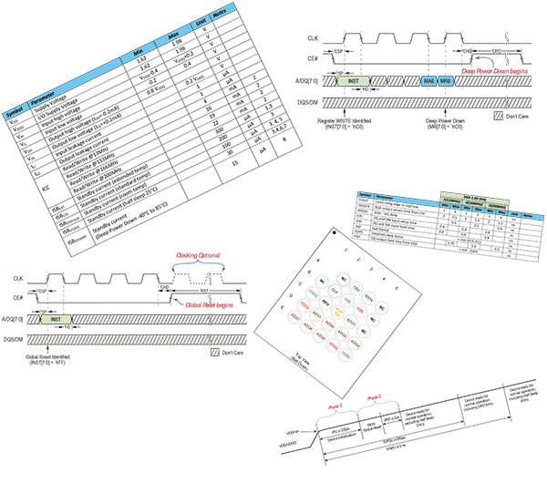
The company has recently announced a game-changing addition to its intellectual property (IP) portfolio: a novel solution that replaces the conventional, often sluggish, SPI (Serial Peripheral Interface) or QSPI (Quad SPI) configuration flash memory commonly used with Field-Programmable Gate Arrays (FPGAs). This new technology leverages a high-speed, low-pin-count, 200 MHz DDR (Double Data Rate) x8 NOR Flash, promising a significant leap forward in FPGA configuration performance and overall efficiency.
This blog post will delve into the details of this innovative solution, exploring its advantages, potential applications, and the impact it’s likely to have on the FPGA landscape. We’ll cover the limitations of existing SPI/QSPI solutions, the benefits offered by the DDR NOR Flash alternative, and the implications for designers and engineers working with FPGAs.
Understanding the Bottleneck: Limitations of SPI/QSPI Configuration Flash
FPGAs are incredibly versatile devices, offering the flexibility to be configured and reconfigured for a wide range of applications. However, this very strength – their programmability – hinges on the speed and efficiency of the configuration process. This process involves loading a bitstream (a file containing the configuration data) into the FPGA’s internal memory. Traditionally, this bitstream is stored in an external non-volatile memory like SPI or QSPI flash.
While SPI and QSPI have served as the de facto standard for FPGA configuration for years, they are not without their limitations:
- Slow Configuration Times: SPI and QSPI are inherently serial communication protocols. They transmit data bit-by-bit, leading to relatively slow configuration times, especially for large bitstreams. This can be a significant bottleneck in applications that require rapid reconfiguration, such as dynamic reconfiguration systems or scenarios where boot-up time is critical.
- Limited Bandwidth: The serial nature of SPI/QSPI also restricts the available bandwidth. This means that the rate at which data can be transferred from the flash memory to the FPGA is limited, impacting the overall performance of the system.
- Pin Count Trade-offs: While SPI offers a low pin count (typically 4-6 pins), QSPI increases the bandwidth by using four data lines. However, this comes at the expense of increased pin count, which can be a constraint in space-sensitive applications.
- Increased Power Consumption: The continuous serial data transfer in SPI/QSPI can contribute to higher power consumption compared to more efficient parallel data transfer methods. This is particularly relevant in power-constrained applications like mobile devices or battery-powered systems.
- Software Overhead: SPI/QSPI communication requires dedicated drivers and software overhead, adding complexity to the overall system design.
These limitations become increasingly pronounced as FPGA designs grow more complex and the size of the bitstreams increase. The result is a bottleneck in the system, hindering performance and potentially limiting the applicability of FPGAs in certain demanding applications.
SLL’s Innovation: A High-Speed DDR NOR Flash Solution
Synaptic Laboratories has addressed these limitations head-on by developing a novel solution based on a high-speed, low-pin-count, 200 MHz DDR x8 NOR Flash. This approach offers a paradigm shift in FPGA configuration, providing significant performance advantages over traditional SPI/QSPI solutions.
Here’s a breakdown of the key features and benefits of SLL’s innovative solution:
- DDR (Double Data Rate) Technology: Utilizing DDR technology doubles the effective data transfer rate compared to standard single data rate (SDR) flash memory operating at the same clock frequency. This significantly improves configuration speed and bandwidth.
- 200 MHz Operating Frequency: The 200 MHz operating frequency further enhances the data transfer rate, allowing for rapid loading of the FPGA configuration bitstream.
- x8 Data Bus Width: The x8 data bus width allows for parallel transfer of 8 bits of data simultaneously, significantly increasing the data throughput compared to the serial transfer of SPI/QSPI.
- NOR Flash Memory: NOR flash offers byte-addressability, meaning individual bytes of data can be accessed directly without having to read an entire block. This facilitates faster and more efficient data access during configuration and other operations.
- Low Pin Count: Despite the increased performance, SLL’s solution maintains a relatively low pin count, making it suitable for applications where space is a premium. This is crucial for integration into smaller form-factor devices and boards.
- Simplified Hardware Design: The integration of DDR NOR flash can often simplify the overall hardware design compared to managing complex SPI/QSPI interfaces, potentially reducing development time and costs.
- Reduced Latency: The faster data transfer rates and byte-addressability of NOR flash translate to reduced latency during configuration, leading to faster boot-up times and improved responsiveness.
Advantages of SLL’s DDR NOR Flash Configuration for FPGAs
The adoption of SLL’s high-speed DDR NOR Flash configuration solution brings a wealth of advantages to FPGA-based systems:
- Dramatically Reduced Configuration Time: The primary benefit is a significant reduction in FPGA configuration time. This allows for faster boot-up times, quicker system initialization, and more responsive dynamic reconfiguration. This is particularly critical in applications like industrial automation, automotive systems, and high-performance computing where rapid startup or reconfiguration is essential.
- Increased System Performance: Faster configuration times translate to improved overall system performance. FPGAs can be rapidly reconfigured to adapt to changing requirements, enabling more dynamic and efficient operation.
- Improved Power Efficiency: While DDR technology itself can consume slightly more power, the significantly reduced configuration time means the system spends less time actively transferring data, potentially resulting in a net reduction in power consumption, especially in applications requiring frequent reconfiguration.
- Enhanced Design Flexibility: The low pin count and simplified hardware design offer greater flexibility in system design, allowing engineers to optimize the placement of components and reduce board size.
- Support for Larger Bitstreams: With the increased bandwidth, SLL’s solution can efficiently handle larger and more complex FPGA bitstreams, enabling the implementation of more sophisticated and feature-rich applications.
- Potential for Over-the-Air (OTA) Updates: The increased bandwidth also makes it easier to implement Over-the-Air (OTA) updates of the FPGA configuration, allowing for remote bug fixes, feature enhancements, and performance optimizations without requiring physical access to the device.
Potential Applications and Industries Benefitting from SLL’s Innovation
The benefits of SLL’s high-speed DDR NOR Flash configuration solution are applicable across a wide range of industries and applications, including:
- Telecommunications: Faster configuration times are crucial for rapid network reconfiguration and adaptation to changing traffic patterns in telecommunications infrastructure.
- Automotive: ADAS (Advanced Driver-Assistance Systems) and autonomous driving applications require real-time processing and rapid adaptation to changing road conditions. SLL’s solution enables faster reconfiguration of the FPGA to handle these dynamic requirements.
- Industrial Automation: Industrial robots and automated systems require rapid reconfiguration to adapt to different tasks and production lines. The faster configuration times provided by SLL’s solution can significantly improve throughput and efficiency.
- Aerospace and Defense: High-performance signal processing and data acquisition systems in aerospace and defense applications demand rapid configuration and high bandwidth.
- Medical Imaging: Medical imaging devices often require real-time processing and rapid reconfiguration to adapt to different imaging modalities and patient conditions.
- Data Centers: FPGA-based accelerators in data centers can benefit from faster configuration times to optimize performance for specific workloads.
- High-Performance Computing (HPC): Applications requiring dynamic reconfiguration of FPGA-based accelerators can benefit significantly from the reduced configuration latency.
- Consumer Electronics: While cost considerations are paramount in consumer electronics, the improved boot-up times and power efficiency offered by SLL’s solution can be valuable in certain applications.
Conclusion: A New Era in FPGA Configuration
Synaptic Laboratories Ltd’s introduction of a high-speed DDR NOR Flash solution for FPGA configuration represents a significant step forward in FPGA technology. By overcoming the limitations of traditional SPI/QSPI flash memory, SLL has paved the way for faster configuration times, improved performance, and enhanced design flexibility. This innovation is poised to revolutionize the way FPGAs are used in a wide range of applications, empowering designers and engineers to create more powerful, efficient, and responsive systems. As FPGA designs continue to evolve and become more complex, solutions like SLL’s will become increasingly crucial for unlocking the full potential of these versatile devices. It will be interesting to see how this technology is adopted and how it influences the future of FPGA-based systems.
SLL is the only specialist, dedicated xSPI SIP design house since 2016. XSPI SIP design and support is SLL core business, for FPGA and ASIC. Visit our website to learn about SLL’s highly innovative xSPI SIP portfolio that is already successfully used by global customers including Fortune Global 500’s, and in 100m+ volume ASIC projects.
Subscribe to our Newsletter
Lorem ipsum dolor sit amet, consectetur adipiscing elit. Ut elit tellus, luctus nec ullamcorper mattis, pulvinar dapibus leo.